| PCBA flow |
Content |
Capacitor |
| Volum |
Solder point |
MOQ |
| PCB size |
200 cm MAX |
| PCB DFM |
Optimize PCB layouts for manufacturability |
| DFT Integration |
Design-for-testability guidance to streamline functional validation |
| Stencil |
General & step stencil |
Laser |
| BOM analysis |
Ready components supply
Future components customization
Substitute for Lyfe cycle end |
Trader 、production 、engineering |
| Samples |
YES |
Samples approval before batch production |
 |
 |
 |
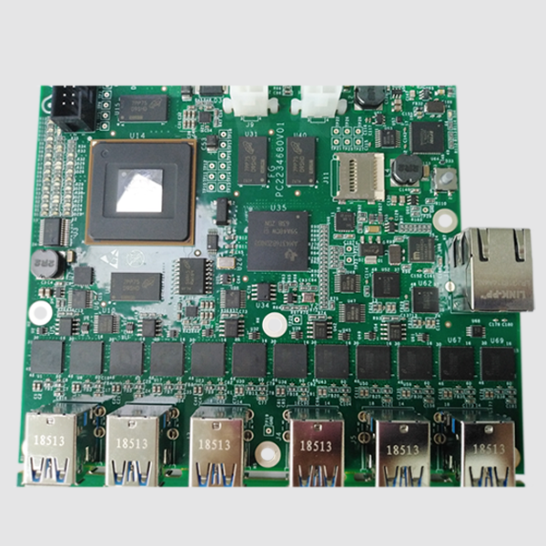
| PCBA |
SMD |
Package size ≥ 01005
Assembly side : top & bottom
QFN : YES
BGA : YES |
| DIP |
Parts assembly before soldering : YES
Ready part for soldering
Assembly side : top & bottom |
| Quality & standard |
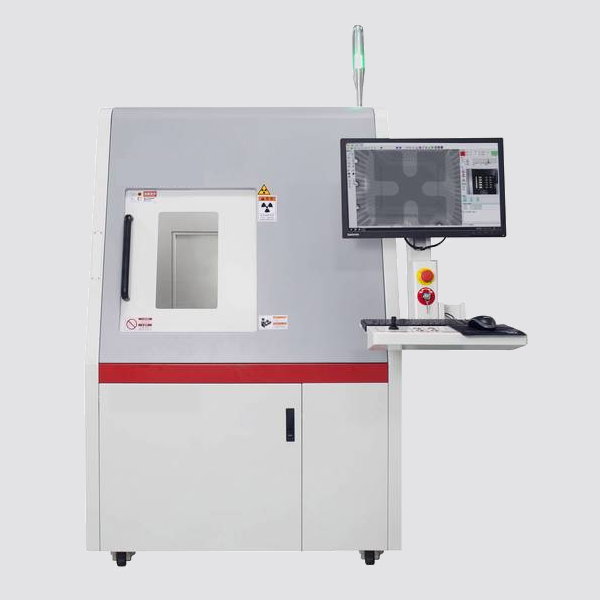
AOI 、functional validation 、Xray & General 、IPC-A-610 Class 2/3 、UL |
|
| PCBA connection |
Hook-up wires |
Solderless terminal , PCB welding |
| Multi-core cables |
Block terminal 、Pluggable block |
PCBA protection
|
Conformal coating |
Thickness ≥50um 、scratch-resistable |
| Heatshrink tube |
Color 、Rohs |
| ABS case |
Modeling 、production 、waterproof IP class |
| Metal sheet |
Aluminum enclosure、waterproof IP class |
| PCBA working |
Programmer |
Single chip / finished products |
| Finished products image |
Packaging box DIY |
Print / spray image with image drawing |
| Product life-cycle managment |
Sustainable supply for BOM |
Risk-free procurement with alternatives pre-qualified for lifecycle and obsolescence. |